Among those who trust us:
Among those who trust us:
The Hidden Cost
Your engineers are capable. The process may not set them up. Ambiguous requirements, features built on untested assumptions, AI initiatives that were never designed for production. These aren't engineering failures. They're upstream gaps that compound with every sprint.
Planorama closes those gaps before they cost you.
Your Challenges
These are the problems we solve every day for organizations building complex software.
Why Planorama
In every engineering discipline, design IS engineering. Only in software is it often relegated as a nice-to-have. Design (done right) defines system behaviors, edge cases, and requirement structures that engineering teams execute against sprint over sprint. We eliminate ambiguity that causes rework, mid-sprint surprises, and features that ship but nobody uses.
AI initiatives often stall in pilot purgatory with POCs that never reach production. We validate feasibility against real user workflows, evaluate models you can actually host, and design governance that clears compliance review. No hype - only AI your engineering team can ship and support.
Companies spend 6+ months hiring and aligning an enterprise design org. We deploy our pre-aligned senior team (no junior handoffs) within days. Your tooling, your backlog, your team. Sign Friday, start Monday.
Engineers see us as peers, not overhead. We hold our own in architectural discussions about multi-tenancy, permissioning, and system trade-offs because we know modern enterprise systems.
Our Services
Schedule a 30-minute call to find out exactly where upstream gaps are costing your engineering team the most.
How We Work
We position ourselves upstream of your engineering sprints and produce the artifacts your developers need before they write a line of code:
Everything we produce becomes permanent institutional knowledge inside your organization. Senior practitioners from day one, and your team carries forward the practices long after the engagement ends.
The artifacts stay.
The way of working stays.
The dependency on us doesn't.
Client Feedback
What you've created saves me hundreds of thousands of dollars a year on development. Your documentation is so detailed that our engineers can implement it right the first time.
I've been doing this for 25 years, and Planorama is the best team I've ever worked with. They're sophisticated and understand the need to create multiple scenarios beyond a simple wireframe.
Their approach to UX design and documentation is way beyond most UX design companies. Our development teams loved it!
Nothing short of amazing work from the Planorama team! The design gets rave reviews every time.
I can count on one half of one hand the number of times I have worked with such a polished and professional firm.
Your documentation is perfect. This is the best feature definition specification I've ever seen.
Is this your documentation? I love this. I want this.
It was an absolute pleasure to work with you all. You made my job easy and were wonderful partners to work with.
With your UX and user stories, I work so much faster.
Your documentation is so streamlined and presents everything I need to code fast.
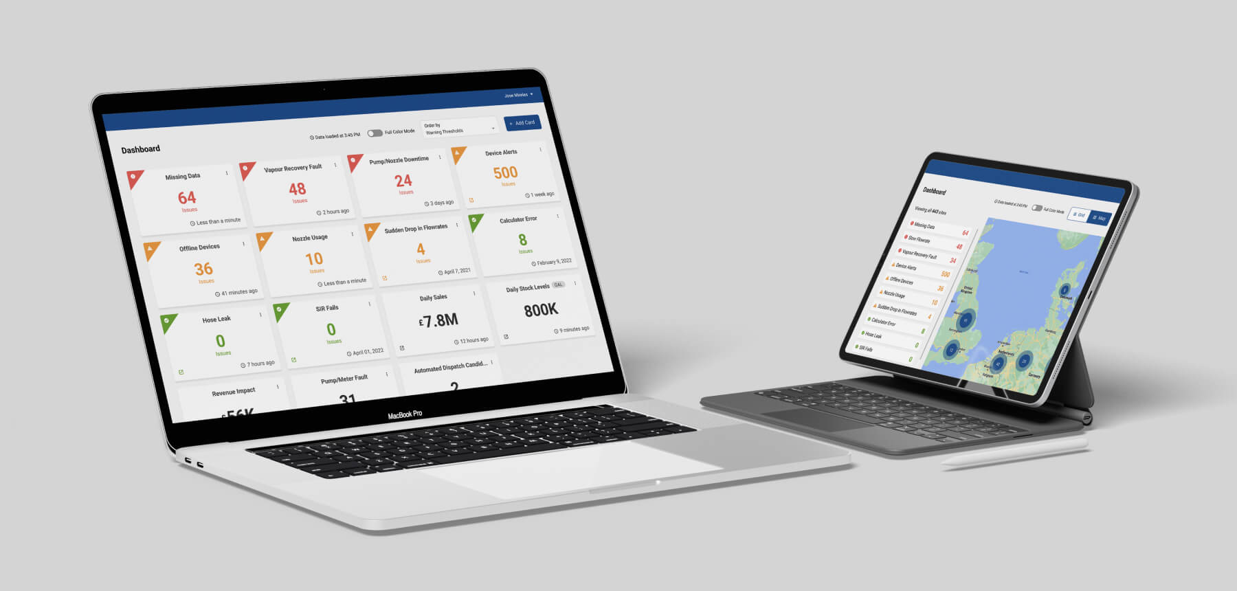
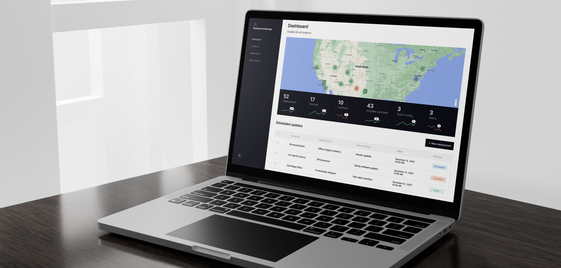
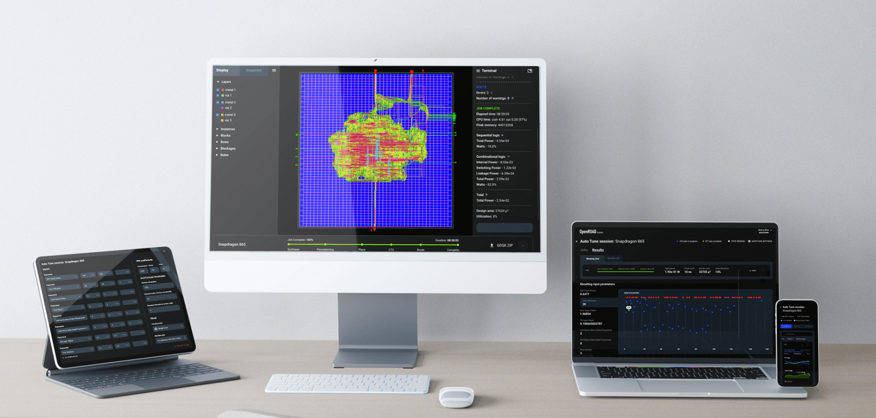
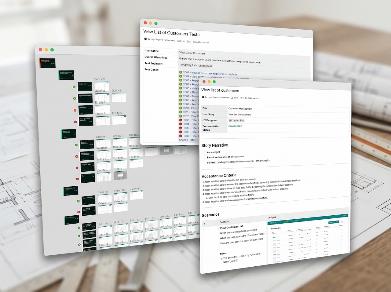
Our Work
Get in Touch
Tell us what you're working on. We'll find where Planorama can have the most impact — and be honest if we're not the right fit.
30-minute discovery call — free, focused, no obligation
Senior practitioners on every engagement, not junior staff
Deliverables your engineers can act on from sprint one
Honest fit assessment — we'll say so if it's not right
Message sent!
We'll be in touch within one business day.